Multiphysics Simulations for Robust Computational Modelling of Stochastic Nanostructures
This work explores the implications of wholly random and non-linear nanostructures on electromagnetic wave propagation within a multiphysics simulation environment. Showcased is a way to noticeably bypass the inaccuracies drawn from the linearity dependency of traditional simulation methods. Applying the COMSOL Multiphysics® software platform, the finite element method and a geometry designed from the ground-up to be variable, the analysis of highly intricate nanostructured material surfaces is uniquely reported.
Employed within the core component of this model was the COMSOL Multiphysics® Wave Optics module configured to provide electromagnetic (EM) wave injection in the frequency domain, opposing the use of the time domain for shorter simulation run time and greater resource efficiency. A Wavelength Domain study step was used in conjunction with a cluster sweep setup to utilise the University of Southampton's IRIDIS 5 supercomputer for rapid parallel computation.
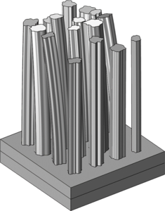
The model used here was expanded on from previous work and not taken from any of the application libraries. It was designed using two types of material domain; one of air and the other of silicon. The silicon and air domains were placed against one-another such that a single interface was formed between them. Perfectly matched layers (PMLs) were then employed to extend these domains infinitely away from the interface between them. A 4-by-4 square grid of silicon nanowires (NWs) could then be created at this interface, extruding outward from the silicon into the air. The air domain was elongated automatically to ensure complete encapsulation of all the NWs within the grid using global parameters.
To create stochastic nanostructures, certain functions with seeded inputs needed to be created to randomise individual parameters of these NWs, such as radius, height, bend and pitch. This means that no pair of NWs can be the same. It is noted how electronic systems can never be truly random and, as such, artificial randomness, or pseudorandomness, needed to be created for each of these parameters. Using random functions, mathematical expressions, static parameters and logical switches, pseudorandomness on a per-NW scale could be achieved for the first time at this level of complexity.
Our results have demonstrated thus far that, by simulating many unit-cells of these random NWs, and then taking an average of their electromagnetic (EM) reflectance, a far more accurate spectral response can be obtained when compared to that of a real, truly random black silicon (b-Si) surface to which the model was based on. The implication is that we can now, far more accurately, simulate heterogeneous nanoscale surfaces whilst also being able to vary the average properties of said surface to identify the global effects on its spectral response characteristics. This is extremely useful for the creation of antireflective materials and coatings for a broad range of applications.