Studies of the Yield of Back-Scattered Electrons in Scanning Field Emission Microscopy
Scanning field emission microscopy (SFEM) is a technique based on Topografiner [1] and Scanning Tunneling Microscopy (STM) [2] technologies. In this work, we do SFEM experiments to measure the electrons emitted by a sharp tungsten tip once they are back-scattered by a W(110) surface with different Fe nano-structures and collected in two electron detectors (called here CLAM2 and Channeltron) located at different positions relative to the microscope.
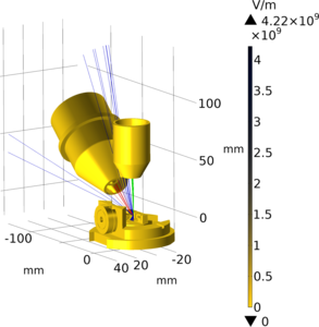
In order to understand geometrical aspects of the collected data we have performed numerical simulations of the trajectory of the secondary electrons yield taking into the account the entire three-dimensional system geometry of our set-up by using COMSOL Multiphysics® software. In Figure 1 it is possible to observe how the electron trajectories (red lines) are bent far from the electrostatic junction forward to the space in between the junction and the detectors when the voltage applied to the tip is increased. For high tip voltages, most of the back-scattered electrons do not achieve the detector’s entrance. This produces the drop behavior of the counts after a certain voltage threshold (plotted in Figure 1d). It must be noticed that the simulations here show the trajectory of the electrons elastically back-scattered only, since they are the most energetic and so the less affected ones by the external electric fields. The results of the simulations allow us to understand that the experimentally observed peak in the spectrum of detected secondary electrons has also a geometric component.
We have used the AC/DC Module for the calculation of the electric potential and electric field in the system and the Charged Particle Tracing Module for the determination of the electron trajectories. Due to the required order of accuracy, it was necessary to use the ECAD Import Module for the definition of the geometry inside of COMSOL Multiphysics® directly from the construction files of the experimental set-up. The simulation is based on the Magnetic Lens model from the Application Libraries.
References
[1] Young, R., Ward, J. & Scire, F. The Topografiner: An Instrument for Measuring Surface Microtopography. Review of Scientific Instruments 43, 999-1011 (1972).
[2] Binning, G., Rohrer, H., Gerber, C. & Weibel, E. Tunneling through a controllable vacuum gap. Applied Physics Letters 40, 178-180 (1982).